Subject:RE: The BEAM clock challenge
Date:Mon, 8 Feb 1999 00:45:55 -0800
From:Wilf Rigter
To:beam@corp.sgi.com
OK, you asked for it!
Here is a way to build a BIOMORPHIC CLOCK and I'm throwing in whole new
family of neurons to Divide and Rule for good measure! But I am afraid you
must read the whole article first before you get to the clock bit and yes,
there will be a quiz at the end (grin). Oh yes, the GIFs are 2K each! OK?
enjoy
Wilf Rigter mailto:wilf.rigter@powertech.bc.ca
----------------------------------------------------------------------------
------------------------------------------------------------------------
2/N NEURONS -
DIVIDE AND MULTIPLY
(c)
wilf rigter Feb 7,1999
INTRODUCTION
The N/2 neuron is presented here as a proof of concept of a spiky stimuli
processing neuron! The N/2 neuron is so named because N/2 is number of
output pulses it generates for every input pulse.
The N/2 neuron has the capability to process spiky inputs and produce spiky
outputs over a wide range of transfer functions that includes INHIBIT,
ATTENUATE, REGENERATE and AMPLIFY. It seems intuitively obvious that
networks of N/2 neurons would be capable of very complex stimuli processing.
Despite of its complex capability, the N/2 neuron is a remarkable simple
circuit.
THE N/2 NEURON MODEL
The neural model of the N/2 neuron is the "programmable spike multiplier".
Input spikes are multiplied at the output by a factor N/2, programmed by the
N/2 neuron internal process time constants. Programming (tuning) of the N/2
neuron is performed by adjusting analog variables which control two internal
process time constants. The ratio of the two process durations determines
the ratio of output to input spikes by a discrete factor of N/2 where N is a
whole number equal to or greater than zero.
The electronic model for the N/2 neuron is the "gated oscillator with
memory". An external negative transition is detected by the edge triggered
Nv input generating an internal gating pulse which enables an internal
oscillator to produce output pulses for the duration of the gating pulse.
The last state of the oscillator output is retained when the gating pulse
terminates. The number of pulses generated for each input pulse is
determined by the ratio of the gating pulse width and oscillator period both
of which are adjusted with analog (RC) components.
While the ratio of analog variable time constants is infinitely
(continuously) variable, the ratio of input to output pulses is a discrete
factor N/2. The first 4 factors of 0/2, 1/2, 2/2 and 3/2 are especially
important since these generate 0, 1/2, 1 and >1 pulses for each input pulse.
The factor of N=0 (0/2) INHIBITS (blocks) the transfer of input pulses. The
factor of N=1 (1/2) ATTENUATES (divides) the transfer of input pulses by 2.
The factor of N=2 (2/2) REGENERATES (but delays) the transfer of input
pulses by 1 ( 1 for 1). The factor of N=3 and higher (3/2 and higher)
AMPLIFIES the transfer of input pulses by N/2.
THE N/2 BINARY COUNTER
The N=1 factor is a special case with an interesting property: N/2 neurons
that can count! The N/2 "divide by 2" (or multiply by 1/2) transfer function
is equivalent to a binary flip-flop and can be cascaded in a linear network
to produce any length neuron ripple counters.
THE N/2 NEURON CIRCUIT
The N/2 neuron consists of three series connected elements:
1. Nv input stage
2. XOR reversing stage
3. Nu output stage.
The N/2 neuron combines an edge triggered input, a polarity control block,
an oscillator, a memory and a local feedback loop. The RC components of the
input and output stages are the analog variables that can be adjusted to
give various time constants. It is the ratio of the Nv and Nu time
constants that determine the transfer function of the N/2 neuron.
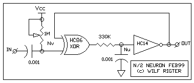 FIG 1 - THE BASIC N/2 NEURON CIRCUIT
As shown in FIG 1, The N/2 neuron external input uses a Nv at one input of a
XOR gate as a "edge triggered" Nervous Neuron to generate a gating pulse.
The output of the XOR gate is connected to an integrating Nu with hysteresis
(memory) and the output of the Nu is the external output of the N/2 Neuron.
The second XOR input is connected to the Nu output to provide positive or
negative feedback with the feedback polarity controlled by the Nv.
Under stable (no process) conditions the XOR provides positive feedback for
the Nu which then behaves as long term memory. When an input pulse occurs,
a Nv process is generated during which the XOR supplies negative feedback to
the Nu which then acts as an oscillator (UniCore). Note the use of
different RC components for the Nv and Nu stages because the thresholds of
HC86 and HC14 are quite different which affects the time constant for the RC
component values. As with most Nv / Nu neuron circuits, the N/2 neuron
requires tuning.
THE N/2 NEURON PROCESS
The example of the N/2 circuit in FIG 1 can be used to demonstrate it's
basic capabilities. The Nv generates an active low gating pulse at the
XOR input at each falling edge of the input waveform. This causes Nu output
to input feedback to change from positive to negative feedback. A Nu with
negative feedback behaves like a classical Schmitt trigger oscillator
alternately charging and discharging the Nu capacitor. with a period
determined by the RC components and the Nu bias point thresholds. Depending
on the ratio of the Nv and Nu "process" time constants (NvTC and NuTC), the
Nu produces 0, 1/2, 1 or more pulses for every negative input transition.
INHIBIT
An active low Nv process connected to one XOR input changes the other XOR
input to output polarity from inverting to non-inverting. This changes the
Nu output to input feedback from positive to negative feedback and causes
the voltage at Nu bias point will start to changing in the direction of the
Nu output polarity. Because of Nu input hysteresis, there is a delay before
the Nu bias point voltage reaches the trigger threshold when the output
changes state. If NuTC is larger than NvTC, the voltage at the Nu bias
point will never reach this threshold before the Nv pulse terminates and the
transfer of input to output pulses is inhibited (blocked) and the output
remains unchanged (N=0).
ATTENUATE
If NuTC is approximately equal to NvTC, the voltage at the Nu bias point
will just cross the threshold and Nu output will change state. Since the
inverted Nu output is connected through the XOR gate back to the Nu input,
the voltage at Nu bias point will start to discharge in the direction of the
Nu new output polarity. Again because of input hysteresis, the Nu output
will not change until the bias point voltage reaches the second threshold.
As long as the Nv gating pulse terminates before the second threshold is
crossed, the Nu output will only change state once. When the Nv pulse
terminates, the XOR gate becomes an inverter in the Nu feedback path and
the bias voltage will charge in opposite direction of the output polarity
thereby holding the Nu output state (memory). On the next falling edge at
the Nv input, the process repeats causing the Nu memory to change state
(flip-flop) on each successive falling edge of the input waveform. As a
result, half of the input pulses are transferred to the output (N=1). If
several stages of N/2 (N=1) neurons, are connected in series, the resulting
network behaves like a binary counter!
REGENERATE
If NuTC is shorter than the NvTC, the voltage at the Nu bias point will
cross the first threshold, causing the Nu output to change state and then
the bias voltage will reverse and cross the second threshold to change the
Nu output state once more. As long as the Nv pulse terminates before the
bias voltage again reaches the first threshold, the Nu output produces one
output pulse for every input pulse. (N=2)
AMPLIFY
If NvTC is much larger than the NvTC, and the voltage at the Nu bias point
crosses thresholds 3 or more times the Nu output will produce 1.5 or more
pulses for every input transition.The transfer of input pulses is AMPLIFIED
when more output pulses than input pulses are generated (N<2)
N/2 NEURON DEMONSTRATION
Unlike it's digital counterpart, the N/2 neuron depends on the ratio of the
analog components for the Nu/Nv time constants to select a transfer
function. In practice this means you can use a photodiode or other sensor to
change one time constant and thereby successively change the transfer
function of the N/2 Neuron from INHIBIT to ATTENUATE, REGENERATE and
AMPLIFY.
To demonstrate the N/2 binary counter example (N=1), we can manually tune
the time constants. Tuning the N/2 neuron for a specific function is
simple. For example to tune the N/2 neuron for N=1 (divide by 2), apply a
pulsing waveform (ie 2Hz microcore pulses) to the 2/N input pin. For the
components shown, the active low input pulses must be >2ms and can be any
frequency below 250 Hz. Higher frequencies can of course be achieved with
different component values. The 1M Nv pot is initially set for minimum and
then slowly adjust the pot until you observe a squarewave at the output
using a LED in series with a 5K resistor between the Nu output and Vcc for
indication. If the pot is adjusted further for smaller TC ratios, the N/2
neuron becomes a quantizing pulse multiplier, producing one output pulse for
each input (N=2=REGENERATE) or 1.5, 2, 2.5, 3, etc output pulses for each
input pulse (N>2=AMPLIFY). Note that the minimum input pulse width must
always be greater than the Nv time constant. Also note that the fractional
output pulses are a combination of a square wave and pulses which will also
cause the LED to blink.
N/2 BIOMORPHIC CLOCK
After tuning the first N/2 neuron to divide by two, measure the resistance
of the variable resistor and wire up the remaining gates (replacing the pot
with fixed resistors) for a total of four N/2 neurons capable of counting 16
input pulses . Any number of N/2 (N=1) neurons can be cascaded to divide the
input frequency by 2 to the nth power. For example 5 chips (2 ea H14 and 3
ea HC86) provide a maximum of 12 neurons which will divide input pulses by
4096. I will design a simple decoder network which will reset an eleven
stage ripple counter network clocked at one minute intervals, when the
counter reaches 1440 (the number of minutes in a day) so that the dream of a
"BIOMORPHIC CLOCK" is realized. Alternately 12 neurons and decoder networks
for count 10, 6, 24 can be used to construct a BIOMORPHIC BCD CLOCK.
Finally, we need some 7 segment decoder networks and a few neural bits to
SET the time.
While this just the beginning of a neural network clock, it is also an
opportunity to get some feedback from the reader!
N/2 COMPLEX NETWORK
I have not yet investigated complex N/2 neural networks that simulate
biological systems although there would appear to be the potential for
implementing complex processing functions using these simple N/2 networks.
While the N/2 neuron circuit works fine in simple networks, there are some
issues that need to be resolved, including normalizing the input and output
pulse widths and pulse spacing required to stabilize the behaviour of N/2
neurons in complex networks. Narrow negative going input pulses will reset
the input Nv before the gating pulse terminates and must be avoided. For a
network of N/2(N=1) neurons this is not a an issue because the neuron output
has a 50% duty cycle. However in multiple input or complex N/2 networks a
minimum pulse width must to be guaranteed at both input and output to ensure
predictable operation. The input pulsewidth can be fixed by adding a second
Nv input stage as shown in FIG 2
FIG 1 - THE BASIC N/2 NEURON CIRCUIT
As shown in FIG 1, The N/2 neuron external input uses a Nv at one input of a
XOR gate as a "edge triggered" Nervous Neuron to generate a gating pulse.
The output of the XOR gate is connected to an integrating Nu with hysteresis
(memory) and the output of the Nu is the external output of the N/2 Neuron.
The second XOR input is connected to the Nu output to provide positive or
negative feedback with the feedback polarity controlled by the Nv.
Under stable (no process) conditions the XOR provides positive feedback for
the Nu which then behaves as long term memory. When an input pulse occurs,
a Nv process is generated during which the XOR supplies negative feedback to
the Nu which then acts as an oscillator (UniCore). Note the use of
different RC components for the Nv and Nu stages because the thresholds of
HC86 and HC14 are quite different which affects the time constant for the RC
component values. As with most Nv / Nu neuron circuits, the N/2 neuron
requires tuning.
THE N/2 NEURON PROCESS
The example of the N/2 circuit in FIG 1 can be used to demonstrate it's
basic capabilities. The Nv generates an active low gating pulse at the
XOR input at each falling edge of the input waveform. This causes Nu output
to input feedback to change from positive to negative feedback. A Nu with
negative feedback behaves like a classical Schmitt trigger oscillator
alternately charging and discharging the Nu capacitor. with a period
determined by the RC components and the Nu bias point thresholds. Depending
on the ratio of the Nv and Nu "process" time constants (NvTC and NuTC), the
Nu produces 0, 1/2, 1 or more pulses for every negative input transition.
INHIBIT
An active low Nv process connected to one XOR input changes the other XOR
input to output polarity from inverting to non-inverting. This changes the
Nu output to input feedback from positive to negative feedback and causes
the voltage at Nu bias point will start to changing in the direction of the
Nu output polarity. Because of Nu input hysteresis, there is a delay before
the Nu bias point voltage reaches the trigger threshold when the output
changes state. If NuTC is larger than NvTC, the voltage at the Nu bias
point will never reach this threshold before the Nv pulse terminates and the
transfer of input to output pulses is inhibited (blocked) and the output
remains unchanged (N=0).
ATTENUATE
If NuTC is approximately equal to NvTC, the voltage at the Nu bias point
will just cross the threshold and Nu output will change state. Since the
inverted Nu output is connected through the XOR gate back to the Nu input,
the voltage at Nu bias point will start to discharge in the direction of the
Nu new output polarity. Again because of input hysteresis, the Nu output
will not change until the bias point voltage reaches the second threshold.
As long as the Nv gating pulse terminates before the second threshold is
crossed, the Nu output will only change state once. When the Nv pulse
terminates, the XOR gate becomes an inverter in the Nu feedback path and
the bias voltage will charge in opposite direction of the output polarity
thereby holding the Nu output state (memory). On the next falling edge at
the Nv input, the process repeats causing the Nu memory to change state
(flip-flop) on each successive falling edge of the input waveform. As a
result, half of the input pulses are transferred to the output (N=1). If
several stages of N/2 (N=1) neurons, are connected in series, the resulting
network behaves like a binary counter!
REGENERATE
If NuTC is shorter than the NvTC, the voltage at the Nu bias point will
cross the first threshold, causing the Nu output to change state and then
the bias voltage will reverse and cross the second threshold to change the
Nu output state once more. As long as the Nv pulse terminates before the
bias voltage again reaches the first threshold, the Nu output produces one
output pulse for every input pulse. (N=2)
AMPLIFY
If NvTC is much larger than the NvTC, and the voltage at the Nu bias point
crosses thresholds 3 or more times the Nu output will produce 1.5 or more
pulses for every input transition.The transfer of input pulses is AMPLIFIED
when more output pulses than input pulses are generated (N<2)
N/2 NEURON DEMONSTRATION
Unlike it's digital counterpart, the N/2 neuron depends on the ratio of the
analog components for the Nu/Nv time constants to select a transfer
function. In practice this means you can use a photodiode or other sensor to
change one time constant and thereby successively change the transfer
function of the N/2 Neuron from INHIBIT to ATTENUATE, REGENERATE and
AMPLIFY.
To demonstrate the N/2 binary counter example (N=1), we can manually tune
the time constants. Tuning the N/2 neuron for a specific function is
simple. For example to tune the N/2 neuron for N=1 (divide by 2), apply a
pulsing waveform (ie 2Hz microcore pulses) to the 2/N input pin. For the
components shown, the active low input pulses must be >2ms and can be any
frequency below 250 Hz. Higher frequencies can of course be achieved with
different component values. The 1M Nv pot is initially set for minimum and
then slowly adjust the pot until you observe a squarewave at the output
using a LED in series with a 5K resistor between the Nu output and Vcc for
indication. If the pot is adjusted further for smaller TC ratios, the N/2
neuron becomes a quantizing pulse multiplier, producing one output pulse for
each input (N=2=REGENERATE) or 1.5, 2, 2.5, 3, etc output pulses for each
input pulse (N>2=AMPLIFY). Note that the minimum input pulse width must
always be greater than the Nv time constant. Also note that the fractional
output pulses are a combination of a square wave and pulses which will also
cause the LED to blink.
N/2 BIOMORPHIC CLOCK
After tuning the first N/2 neuron to divide by two, measure the resistance
of the variable resistor and wire up the remaining gates (replacing the pot
with fixed resistors) for a total of four N/2 neurons capable of counting 16
input pulses . Any number of N/2 (N=1) neurons can be cascaded to divide the
input frequency by 2 to the nth power. For example 5 chips (2 ea H14 and 3
ea HC86) provide a maximum of 12 neurons which will divide input pulses by
4096. I will design a simple decoder network which will reset an eleven
stage ripple counter network clocked at one minute intervals, when the
counter reaches 1440 (the number of minutes in a day) so that the dream of a
"BIOMORPHIC CLOCK" is realized. Alternately 12 neurons and decoder networks
for count 10, 6, 24 can be used to construct a BIOMORPHIC BCD CLOCK.
Finally, we need some 7 segment decoder networks and a few neural bits to
SET the time.
While this just the beginning of a neural network clock, it is also an
opportunity to get some feedback from the reader!
N/2 COMPLEX NETWORK
I have not yet investigated complex N/2 neural networks that simulate
biological systems although there would appear to be the potential for
implementing complex processing functions using these simple N/2 networks.
While the N/2 neuron circuit works fine in simple networks, there are some
issues that need to be resolved, including normalizing the input and output
pulse widths and pulse spacing required to stabilize the behaviour of N/2
neurons in complex networks. Narrow negative going input pulses will reset
the input Nv before the gating pulse terminates and must be avoided. For a
network of N/2(N=1) neurons this is not a an issue because the neuron output
has a 50% duty cycle. However in multiple input or complex N/2 networks a
minimum pulse width must to be guaranteed at both input and output to ensure
predictable operation. The input pulsewidth can be fixed by adding a second
Nv input stage as shown in FIG 2
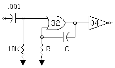
 FIG 2 - N/2 NEURON WITH INPUT PULSE SHAPING
Subject:N/2 NEURONS
Date:Mon, 15 Feb 1999 03:27:38 -0800
From:Wilf Rigter
To:beam@corp.sgi.com


Back by popular demand and full of corrections and latest developments, here
is the article on the N/2 NEURON. I send most of this info to Mark T. and
the Zoz but while the latter came back with some nice comments including the
XOR BEAM anathema which spurred the ELEMENTAL N/2 design , the former
appears to be "incommunicado". Still right across the hall from each other
eh! (yes am canadian). So without the benefit of the master's comments but
looking forward to all your "questions" here is the article.

enjoy

wilf


N/2 NEURONS - MULTIPLY AND DIVIDE (c) wilf rigter Feb 14,1999

INTRODUCTION

The N/2 neuron is presented here as a proof of concept of a spiky stimuli
processing neuron! The N/2 neuron is so named because N/2 is represents the
ratio of 1/2*N output pulses for every input pulse.

The N/2 neuron has the capability to process spiky inputs  and produce spiky
outputs over a wide range of transfer functions that includes INHIBIT,
ATTENUATE, REGENERATE and AMPLIFY.  It seems intuitively obvious that
networks of N/2 neurons would be capable of very complex stimuli processing.
Despite of its complex capability, the N/2 neuron is a remarkable simple
circuit.

THE N/2 NEURON MODEL

The neuron model of the N/2 neuron is the "programmable spike multiplier" .
Input spikes are multiplied at the output by a factor N/2, programmed by the
N/2 neuron internal process time constants. Programming (tuning) of the N/2
neuron is performed by adjusting analog variables which control two internal
process time constants.  The ratio of the two process durations determines
the ratio of output to input spikes by a discrete factor of N/2 where N is a
whole number equal to or greater than zero.

The electronic model for the N/2 neuron is the "gated oscillator with
memory". An external  negative transition is detected by the edge triggered
Nv input generating an internal gating pulse which enables an internal
oscillator to produce output pulses for the duration of the gating pulse.
The last state of the oscillator output is retained when the gating pulse
terminates. The number of pulses generated  for each input pulse is
determined by the ratio of the gating pulse width and oscillator period both
of which are adjusted with analog (RC) components.

While the ratio of analog variable time constants is infinitely
(continuously) variable, the ratio of input to output pulses is a discrete
factor N/2.  The first 4 factors of 0/2, 1/2, 2/2 and 3/2 are especially
important since these generate 0, 1/2, 1 and >1 pulses for each input pulse.


The factor of N=0 (0/2) INHIBITS (blocks) the transfer of input pulses.

The factor of N=1 (1/2) ATTENUATES (divides) the transfer of input pulses by
2.

The factor of N=2 (2/2) REGENERATES (but delays) the transfer of input
pulses by 1 ( 1 for 1).

The factor of N=3 and higher  (3/2 and higher) AMPLIFIES the transfer of
input pulses by N/2.

THE N/2 BINARY COUNTER

The N=1 factor is a special case with an interesting property: N/2 neurons
you can count on!  The N/2 "divide by 2" (or multiply by 1/2) transfer
function is equivalent to a binary flip-flop and can be cascaded in a linear
network to produce any length neuron ripple counters.

THE XOR N/2 NEURON

There are a number of N/2 neuron circuits which behave in similar ways:

The XOR N/2 neuron consists of three series connected elements:

1. Nv input stage
2. XOR reversing stage
3. Oscillator output stage.

The XOR N/2 neuron combines an edge triggered input, a polarity control
block, a Nu and a local +/- feedback loop. The RC components of the input
and output stages are the analog variables that can be adjusted to give
various time constants.  It is the ratio of the Nv and Nu time constants
that determine the transfer function of the N/2 neuron.


Vcc_______     ________________________________
    |     |   |  XOR              Nu           |
    +-->[1M]  |    __                    __    |
          |   +--))86 \_            ____|14 \__|__ OUT
IN  ---||-+------))__ / `--[330K]--|    |__ /
      .001 Nv                      |
                              .001===
                                   |
                                  0V

FIG 1 - THE XOR N/2 NEURON CIRCUIT)

As shown in FIG 1, The N/2 neuron external input uses a Nv at one input of a
XOR gate as a "edge triggered" Nervous neuron to generate a gating pulse.
The output of the XOR gate is connected to an Nu neuron and the output of
the Nu neuron is the external output of the N/2 Neuron. The second XOR input
is connected to the Nu output to provide positive or negative feedback with
the feedback polarity controlled by the Nv. Under stable (no process)
conditions  the XOR provides positive feedback for the Nu which then behaves
as long term memory. When an input pulse occurs, a Nv process is generated
during which the XOR supplies negative feedback to allow the Nu to cycle
(Schmitt oscillator).  Note the use of different RC components for the Nv
and Nu stages because the thresholds of HC86 and HC14 are quite different
which affects the time constant for the RC component values. As with most Nv
/ Nu neuron circuits, the XOR N/2 neuron requires tuning.


THE  2XOR N/2 CIRCUIT

A similar approach can be used with a gated CMOS oscillator normally
constructed with two inverters (see FIG 3). When the inverters are replaced
with non-inverting stages the circuit acts as a memory. The internal gating
pulse on the XOR inputs control whether the XORs are inverting or not. It
may be necessary to add a small (.001) capacitor to the OUTPUT to clean up a
glitch at the end of the Nv period because of slightly different thresholds
of the 2 XOR stages.


Vcc________    __________________||_______||__ 0V
    |     |   |                  ||     | ||
    |     |   |--[500K]---+     .01     | .001
    +-->[1M]  |    __     |             |
     .01  |   +--))86 \___|      __     |
IN ___||__|------))__ /    `---))86 \ __|__ OUTPUT
      ||   `-------------------))__ /

FIG 2 - THE 2XOR N/2 NEURON

The N/2 circuits in FIG 1 and FIG 2 use XOR gates, for which there are no
simple equivalents in biological systems and which are considered to be too
"digital" by some (apparently including Mark T.)


THE ELEMENTAL N/2 NEURON

The last N/2 neuron circuit is in that sense more biomorphic! It is designed
with the simplest of all circuit elements avoiding all trappings of digital
logic. The active components could in theory be reduced to the equivalent of
3 or 5 transistors. The ELEMENTAL N/2 NEURON consists of three series
elements.

1. Nv input stage
2. Bilateral switch
3. Nv Oscillator

The ELEMENTAL N/2 NEURON uses two each resistors, capacitors, inverters and
a single bilateral switch to form the gated oscillator/memory circuit. Since
the input switching thresholds of these devices is symmetrical and near
Vcc/2, the switching symmetry and time constants of the Nv input and the Nv
oscillator stages are close in their characteristics and relatively stable
with variations in Vcc. The other advantage of the ELEMENTAL N/2 NEURON is
the reset of the capacitor charge when no process is active (Bilateral
switch is closed).  This means that every active process starts from zero
capacitor charge which is precisely the same condition for a freerunning Nv
oscillator at the start of each half cycle. As a result, the N/2 ratio pulse
multiplying transfer functions of the N/2 change linearly with RC values and
maintains a robust predictable relationship between the functions and
component values  and eliminates empirical "tuning"!
The ELEMENTAL N/2 NEURON circuit is shown in FIG 3.

           Vcc                __
            |        _____ __|04 \___
            |       |     |  |__ /   |
          [100K]    |     |_         |
            |R1     |     | `-[100K]-|
 IN ____||__|______/     ===    R2   |____ OUT
        ||        / 4066  |   __     |
        .01         |_____|__/04 |___|
                             \__ |

FIG 3 - THE ELEMENTAL N/2 NEURON

THE N/2 NEURON PROCESS

The examples of the two N/2 circuit in FIG 1 and 2 can be used to
demonstrate the basic N/2 capabilities. The Nv generates an active low
gating  pulse at the input at each falling edge of the input waveform which
enables the oscillator process and depending on the duration of the Nv input
process (NvTC) and the oscillator process (XTC), the output will generate
0,1/2,1,1.5,2, etc output pulses for each negative input transition.

The XOR N/2 NEURON PROCESS

In the case of the XOR N/2 neuron, the gating pulse causes the oscillator
output to input feedback to change from positive to negative feedback. An
integrator followed by a Schmitt trigger with negative feedback is a
classical Schmitt trigger oscillator alternately charging and discharging
the oscillator capacitor with a period determined by the RC components and
the Schmitt trigger input thresholds. Note that the initial oscillator
process starts at 0V or Vcc and therefore has a much larger timeconstant
than the subsequent processes which oscillate between the trigger
thresholds. Depending on the ratio of the Nv and oscillator "process" time
constants (NvTC and XTC),  the oscillator produces 0, 1/2, 1 or more pulses
for every negative input transition.  For example: An active low Nv process
connected to one  XOR input changes the other XOR input to output polarity
from inverting to non-inverting. This changes the Nu output to input
feedback from positive to negative feedback and causes the voltage at Nu
bias point will start to changing in the  direction of the Nu output
polarity. Because of Nu input hysteresis,  there is a delay before  the Nu
bias point voltage reaches the trigger threshold when the output changes
state.  If XTC is larger than NvTC, the voltage at the Nu bias point will
never reach this threshold before the Nv pulse terminates and the transfer
of input to output pulses is inhibited (blocked) and the output remains
unchanged (N=0). Longer NvTC periods permit the bias point voltage to cross
the threshold and the Schmitt trigger output to reverse one or more times.
This results in the various N/2 transfer functions described in more detail
below.

The ELEMENTAL 2/N NEURON PROCESS

In the case of the ELEMENTAL N/2 neuron a negative transistion on the NV
input generates an active low gating pulse which turns off the bilateral
switch. This starts the Nv input time constant with zero charge on the input
capacitor which then charges up through the input resistor to Vcc. During
that time the bilateral switch is open and the Nv oscillator process starts
with zero charge on the oscillator capacitor (like the Nv input capacitor)
which charges towards 0V or Vcc depending on the state (memory) of the last
process. The processes of the Nv input and Nv oscillator are very similar
and if the switching thresholds are near Vcc/2 then these two processes are
symmetrical and effects of temperature and voltage variations tend to cancel
out.

INHIBIT

When the time constant of the Nv input (NvTC) is shorter than the time
constant for the first oscillator half cycle (XTC) then the oscillator will
return to it's starting state when the Nv process terminates and no change
in N/2 neuron output will result.  As a result no input pulses will reach
the output so the N/2 neuron is said to be blocked or inhibited (N=0)

ATTENUATE

If XTC is approximately equal to NvTC, the voltage at the oscillator bias
point will just cross the threshold and oscillator output will change state.
The inverted output then starts to charge the capacitor in the direction of
the new output polarity. The oscillator output will not change until the
bias point voltage reaches the second threshold. As long as the Nv gating
pulse terminates before the second threshold is crossed, the oscillator
output will only change state once.  When the Nv pulse terminates positive
feedback will hold the last oscillator output state (memory). On the next
falling edge at the Nv input, the process repeats causing the
oscillator/memory to change state  (flip-flop) on each successive falling
edge of the input waveform. As a result, half of the input pulses are
transferred to the output (N=1). If several stages of N/2 (N=1) neurons, are
connected in series, the resulting network behaves like a binary counter!

REGENERATE

If XTC is shorter than the NvTC, the voltage at the Nu bias point will cross
the first threshold, causing the oscillator output to change state and then
the charging voltage will reverse and the bias voltage will cross the second
threshold to change the oscillator output state once more. As long as the Nv
pulse terminates before the bias voltage again reaches the first threshold,
the oscillator output produces one output pulse for every input pulse. (N=2)


AMPLIFY

If XTC is much larger than the NvTC, and the voltage at the oscillator input
voltage crosses thresholds 3 or more times, the oscillator output will
produce 1.5 or more  pulses for every input transition.The transfer of input
pulses is AMPLIFIED when more output pulses than input pulses are generated
(N>2)

N/2 NEURON DEMONSTRATION

Unlike it's digital counterpart, the N/2 neuron depends on the ratio of the
analog components for the Oscillator/Nv time constants to select a transfer
function. In practice this means you can use a photodiode or other sensor to
change one time constant and thereby successively change the transfer
function of the N/2 Neuron from INHIBIT to ATTENUATE, REGENERATE and
AMPLIFY.

To demonstrate the N/2 binary counter example (N=1), we can manually tune
the time constants.  Tuning the N/2 neuron for a specific function is
simple. For example to tune the N/2 neuron for  N=1 (divide by 2), apply a
pulsing waveform (ie 2Hz MicroCore pulses) to the 2/N input pin. For the
components shown,  the active low input pulses must be >2ms and can be any
frequency below 250 Hz. Higher frequencies can of course be achieved with
different component values.  The 1M Nv pot is initially set for minimum and
then slowly adjust the pot until you observe a squarewave at the output
using a LED in series with a 5K resistor between the output and Vcc for
indication. If the pot is adjusted further for smaller TC ratios, the N/2
neuron becomes a quantizing pulse multiplier, producing one output pulse for
each input (N=2=REGENERATE) or 1.5, 2, 2.5, 3, etc output pulses for each
input pulse (N>2=AMPLIFY). Note that the minimum input pulse width must
always be greater than the Nv time constant. Also note that the fractional
output pulses are a combination of a square wave and pulses which will also
cause the LED to blink.

N/2 BIOMORPHIC CLOCK

After tuning the first N/2 neuron to divide by two, measure the resistance
of the variable resistor and wire up the remaining gates (replacing the pot
with fixed resistors) for a total of four N/2 neurons capable of counting 16
input pulses . Any number of N/2 (N=1) neurons can be cascaded to divide the
input frequency by 2 to the nth power.  For example 5 chips (2 ea. H14 and 3
ea. HC86) provide a maximum of 12 neurons which will divide input pulses by
4096. I will design a simple decoder which will reset an eleven stage
counter chain clocked at one minute intervals, when the counter reaches 1440
(the number of minutes in a day) so that the dream of a "BIOMORPHIC CLOCK"
is realized. Alternately 12 neurons and decoders for 10, 6, 24 can be used
to construct a BIOMORPHIC BCD CLOCK.  Remember that these are "ripple"
counters and a 1ms delay (settling time) is introduced at  each stage. This
limits the input frequency and/or limits the maximum length of the network
just like digital ripple counters .


MONO N/2 NEURON

While the N/2 neuron circuit works fine in simple networks, there are some
issues that need to be resolved, including normalizing the input and output
pulse widths and pulse spacing required to stabilize the behaviour of N/2
neurons in complex networks.  Narrow negative going input pulses will reset
the input Nv before the gating pulse terminates and must be avoided. For a
network of N/2(N=1) neurons this is not a an issue because the neuron output
has a 50% duty cycle.
However in multiple input or complex N/2 networks a minimum pulse width must
to be guaranteed at both input and output to ensure predictable operation.
The input pulsewidth can be fixed by adding one more Bilateral switch at the
input stage as shown in MONO N/2 NEURON in FIG 4 .  This switch isolates the
IN terminal from the Nv capacitor after the Nv is triggered by an active low
transition and for the duration of the NvTC uses R1 to hold the IN side of
the cap low. After the voltage across R2 is equal to Vcc/2, the 4066 switch
turns on to reconnect the IN to the cap after the Nv times out. Resistor R1
provides a "low" impedance current path for charging CNv while the IN
terminal is isolated. The voltage drop across R1 introduces a small error in
the NvTC and the value of R2 should be at least 20 times the value of R1 to
minimize this error.  Note the use of "elementary" (non-digital) components
for this non-retriggerable Nv monostable circuit. I am presently exploring
if an output pulse Nv is required for cascading Amplifying N/2 stages.


      0V        Vcc                __
      |         |        _____ __|04 \___
      |         |       |     |  |__ /   |
    [10K]      [1M]     |     |_         |
      |R1       |R2     | .001| `--[1M]--|
      |____||___|______/     ===    R3   |____ OUT
      |    ||   |     / 4066  |   __     |
      |   .001  |       |_____|__/04 |___|
        /_______|                \__ |
               /
             |
            IN

FIG 4 - THE ELEMENTAL MONO N/2 NEURON WITH FIXED GATING PULSE


COMPLEX N/2 NEURAL NETWORKS

I have not yet investigated complex N/2 neural networks that simulate spiky
neuron biological systems although there would appear to be the potential
for implementing processing functions using these simple N/2 networks. While
not needed for N/2 in the N=0 to 2 modes, it appears that a network of
AMPLIFYING (N>2) N/2 neurons require an output conditioning to generate
fixed width output pulses.
The design objective is that one pulse cascading through several linearly
connected (1 dimensional) stages of  N/2  neurons in the AMPLIFY mode would
produce a saturated pulse train with continuous equally spaced pulses of
2NvTC period. If the saturated pulse train encounters an N/2 neuron in the
ATTENUATE mode the pulse train would be divided by 2. Several stages of
attenuation will increase the interval between pulses and an INHIBIT mode
neuron would block any pulses. In 2 dimensional networks of N/2 neurons in
the AMPLIFY mode, a hemispheric wave of pulses would propagate from the
single initiating pulse with the wavefront washing around groups of N/2
neurons in the ATTENUATE and INHIBIT mode.

NEURAL NETWORK SIMULATOR AND STATUS DISPLAY

I have just started to read about the Cellular Automata (CA) work of
TOFFOLI. Several CA synthesizers programs (including JC) are available for
the PC and are apparently in the public domain. These CA are like arrays of
virtual BEAM machines (reproduction by any electronic means prohibited?) The
process of each cell is determined by simple rules and the new states of the
cell are calculated at each tick of the clock.

It may be possible to program the rule table for these CA programs to
simulate N/2 neural networks. In any case an analog simulator would be very
useful to test some of these ideas.  I can't afford the specialized CA
computing engines which are not the large scale arrays of silicon CA I had
anticipated but instead seem to be RULE engines connected to memory planes
with pipelines to video output. These CA engines like the CAM6 plug into a
PC to generate 256x256 multicolor displays of CA using multi plane neighbor
rule tables at ~60 frames/sec. ( I hope I got most of that right - anyone
out there more familiar with the details?)

If a virtual MicroCore can be programmed into a PIC (which I'm sure it can
be), it should be possible to write a program for the PC that simulates one
, several, hundreds of photovore poppers, walkers,  I wonder....

                Wilf Rigter     mailto:wilf.rigter@powertech.bc.ca
Subject:BEAM - TECHNOLOGY OF EVOLUTION
Date:Wed, 17 Feb 1999 23:49:56 -0800
From:Wilf Rigter
To:"'M le Roux'" , beam@corp.sgi.com


Hello Juan,

You bring up an important point. I think that BEAM robot "survivability" has
been consciously isolated from BEAM "applications".   Read Living Machines
and then make up your own mind.

The following  are my own opinions and based in part on my reading of the
literature and the opinions of others. They are also an extrapolation of
the more conventional explanations of  BEAM technology.

                           The Technology of Evolution
                               wilf rigter (c) 1999


In the technology of evolution we focus our attention on the fundamental
problems of  emulating biological evolution with technological evolution.

The technology that follows bears a resemblance to biological systems but is
not a "copy" of  biological systems. The emphasis on evolution in
development of BEAM technology, is sharply different from other design
philosophies which views legacy technologies only in terms of "problems of
backward compatibility" to be phased  out as soon as possible. This reduces
the range of evolutionary pathways through a process of fossilization of
technological history both in the technology itself and the minds of it's
creators.

Take the case designing a robot walker with a electromechanical system based
on biological legs.

There are two distinctly different approaches to this problem.

1. Reverse engineering
2. Evolutionary design

Reverse engineering decomposes the form and function of  "biological legs"
into subsystems (skeleton, muscle, circulation and nervous system) and
further down into "components" (bone, connective tissue, blood, neurons )
and "elements" (ATP, ion channels) but I'm regressing . Next equivalent
electronic/mechanical components and subsystems are found and are combined
into a walker design which is then optimized to resemble "biological legs"
as close as possible.
It may be said that in this engineering philosophy form is derived from it's
function (ie application).

In biological systems, the evolution of legs can be traced as a series of
adaptations starting with mobile multicellular organisms in the primordial
oceans increasing their access to food/energy through mobility to Ben
Johnson increasing his access to money/energy in the 100 yd dash. Despite
specialization of human legs for walking they retain other secondary
functions such as climbing, swimming, kicking, crushing, curling up and
picking up pencils from the floor. Legs in other species are specialized in
different ways like running, climbing, paddling etc but also have a range of
secondary functions. In general, despite apparent specialization,
"biological legs" represent and retain the memory of their evolutionary
process. Biological "legs" are remarkably versatile and adaptive to the
current environments and retain the ability to evolve into new niches.

The evolutionary design approach is acutely aware that biological systems
are not  "designed" but are instead a snap shot of an ongoing adaptive
process common to all life.

Therefore the evolutionary machine design duplicates natural evolution in an
iterative process of inventing  primitive electro/mechanical elements and
subsystems whose adaptation to the environment and reproductive success is
based not on sex but on survival of the fittest technology (may the best
tech win). The most successful of these  elements and subsystems are then
successively combined into higher and more complex systems culminating in
"useful" applications similar to species evolved in to ecological niches.
One could argue that in evolution  "function follows form"  since adaptation
is largely a series of mutations of form with emergent functions that favor
survival.
As a result the current batch of "walkers" have "legs" and  mimic insectoid
forms in their mode of locomotion. But the basic BEAM "walker" mechanisms
are discoveries as much as designs and are quite unique and potentially
broad in their applications.

This is the exciting characteristic of the evolutionary design approach: we
don't know exactly what we are designing. It's much more a process of
discovery and invention rather than engineering.

So BEAM technology as a form of evolutionary design  is barely off the
starting block in terms of it's own evolution, however within a few thousand
generations (about 10 yrs with a focused group effort of people  building
and trying out designs)  BEAM's "sum over histories" phase space will have
increased by several orders magnitudes and I would expect the fundamental
forms and functions of advanced BEAM organisms to have  much more in common
with the  self-similarity and adaptive mechanisms of living biological
organism than with computers. Then BEAM  applications can be "filled" by
nudging a branch of  BEAM  ecology into the "application niche". At that
time BEAM can truly lay claim to be the technology of LIVING MACHINES.

Although BEAM function follows form and we would like to see  our BEAM
creations reach their full evolutionary potential, some ethical constraints
must be imposed on our own involvement in this process based on the Asimov's
laws of robotics. Despite the importance of  "survival" at this stage in
BEAM evolution we should note that our own survival as a species comes first
("zeroth law") and that survival of the robot is the subservient third law.
If we are successful at facilitating the evolution of "living machines"  we
may also have created  potential competitors for our own species! So I say
to you, "Observe Asimov's Laws and please do not permit the evolution of
self-replicating carnivorous living machines especially if they are great
survivors"


                Wilf Rigter     mailto:wilf.rigter@powertech.bc.ca


> -----Original Message-----
> From: M le Roux [SMTP:mleroux@itec.co.za]
> Sent: Monday, February 15, 1999 3:20 PM
> To:   beam@corp.sgi.com
> Subject:      Re: hmmm...i wonder which subject
>
> >Having a bot take on a job is a little over the current state of BEAM
> >robotics, and is not really keeping in tune with the general "bottom up"
> >approach..We aren't trying to make a bot that can get from point A to
> >point B so that it can accomplish a set goal. The BEAM/bottom up
> >approach is to make a bot that can start from point A and *not get
> >itself killed* without even trying to get to point B..
>
>
> How will we know when we have reached this objective?
> Surely the required level of surviveability depends on the intended
> application?
> I agree that one of the fundamental aspects of BEAM is
> surviveability, but I don't think is should be an isolated (or
> exclusive)goal. We will only be limiting ourselves.
>
> It should rather be seen as an integral (and important) part of a larger
> and
> more far-sighted design process. (not a hurdle to be overcome before any
> further development can take place)
>
> Being new to BEAM and the list, I hope I'm not being too presumptuous :)
>
> Juan
Subject:Re: associative memories
Date:Sun, 21 Feb 1999 15:51:38 -0800
From:Sean Rigter
To:Noam Rudnick , beam


Wilf Rigter wrote:

>What's the question?

Noam Rudnick wrote:

>Good question!

Hi Noam,

I'm a bit out of my element when it comes to the details of associative
memory networks but I can sketch out requirements and a possible
mechanism for such networks based on intuition and common sense (maybe
others higher up on the learning curve could help):

> At what point does it become impossible to hold any more
> memories? Never?

The amount of data you can store  will depend on the configuration
(number of nodes and layers of the associative memory (AM) network. The
larger the number of nodes the higher the resolution of the decision
process.

>I was thinking more like visual memories.

Let's say you have a bot with an AM network with inputs connected to a
visual matrix of 16 photo sensors. backup control of the bot. In this
simple case the sensors are either on or off dependent on the light
level of each sensor and the thresholds. In addition there is a  "learn"
input which is connected to a "danger" sensor. The "danger" signal
occurs for example when sensing high current drain indicating someone's
robbing your energy stores (or you've just fallen into the ocean or your
motors are stalled). To make the AM useful and do something in response
to danger, an output is connected to the bot's reverse motion control.

Anyway the idea is to have a circuit which can be trained with visual
patterns which represent danger conditions and which can be avoided by
backing up. After sufficient "experience", a visual pattern similar to
the danger condition produces an output which backs up the bot before
the danger signal itself is triggered (anticipation/avoidance).

The AM network's association of a visual pattern with a "danger
response" (run away!) comes from the learned "pathways" between input
and the output layers.

So imagine a AM network 16 bits (nodes) wide and 16 layers deep for a
total of 256 AM nodes. The visual input is a 16 bit word that is applied
to the network input layer. Whenever a "danger" condition occurs, each
network layer are "updated". The input layer with the output of the 16
bit visual matrix and the next layer with the state of the prior layer.
This means that the nodes in each layer change state depending on the
state of the inputs to the node including their current state
(feedback), the state of their "lateral neighbours" (weight/threshold),
and the state of the upstream layer nodes (feedforward).  Therefore the
network nodes in various layers are turned on or off depending on the
history of all previous "danger" events establishing a pathway for
matching patterns to reach the output layer to turn on the "reverse"
control signal.
So the network now responds to patterns which closely match previous
patterns associated with danger and produce a corresponding "reverse"
output signal.

>(to paraphrase Noam): In order to associate two visual patterns is this
>just a matter of adjusting the resistances between each neuron?

Yes and no. Adjusting weighting factors between AM nodes is part of the
filtering process that sorts the information from the noise or tailors
the response of the AM to information but after filtering, the
information itself is learned and stored in the network node memories.

The remembered pathway becomes the "function" of the network to
propagate visual patterns to the output layer when the patterns closely
match previous patterns remembered at danger time in the previous
example.
To associate 2 patterns and initiate the same response, the "danger"
signal can be replaced with the output of another network which
remembers a different pattern with a response. So when the pattern in
network A is present at it's inputs, the pattern at the network B inputs
is propagated into the B network associating the B pattern with the A
pattern and output.

The filtering ( weighting) is needed to concentrate information content.
Since there may be random visual patterns (noise) at danger time which
don't add to useful information to the AM network, additional input
layer processing can be used to increase the "information to noise
ratio". For example, a logical function (weighing factor) at the pattern
inputs can be used to permit "mostly significant" patterns such as
visual edges or repeating patterns like stripes to propagate pathways to
the output layer.

The end result is an AM network which can recognize visual input
patterns through a process of learning and initiates avoidance control
based on the patterns' association with "danger".

> I hope these examples cleared up any misundersatndings about my original
> question.

Yes! The answers are as good as the examples and questions of the guy
who is asking and the knowledge of the guy who is answering.

So: excellent examples and questions but warning: I'll now go and read
the literature and find out if I'm even close  8^)
 enjoy
Wilf Rigter mailto:wilf.rigter@powertech.bc.ca
enjoy
Wilf Rigter mailto:wilf.rigter@powertech.bc.ca enjoy
wilf
enjoy
wilf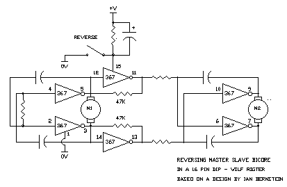 Ian Bernstein wrote:
> You could easily get two bicores and one reverser into one 74xxx240.
>
> *-_-_-_-_-_-_-_-_-_-_-_-_-_-_-_-_-_-_-_-_-_-_-_-_-_-_-_-_-_-_-_-*
> Ian Bernstein "aka - Synet" The Master Builder
Ian Bernstein wrote:
> You could easily get two bicores and one reverser into one 74xxx240.
>
> *-_-_-_-_-_-_-_-_-_-_-_-_-_-_-_-_-_-_-_-_-_-_-_-_-_-_-_-_-_-_-_-*
> Ian Bernstein "aka - Synet" The Master Builder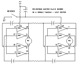 enjoy
wilf
enjoy
wilf